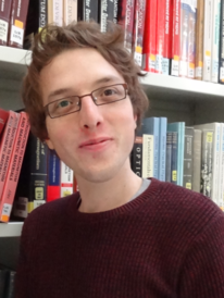
Peter Griffin

Peter talks about his experience of the group after just a few months.
Download Peter's researcher profile as a pdf.
Contact details and more information on Peter's research
How did you join the Cambridge Centre for Gallium Nitride?
I first heard about the GaN group from a presentation by Rachel Oliver on whispering gallery modes in a GaN disc resonator. The talk was part of the introduction week to the joint UCL and Cambridge Doctoral Training Centre in integrated photonic and electronic systems, which I am registered on. I talked to Rachel after the talk and was really excited by the work she was doing. From this first point of contact we later wrote a proposal together for the mini-project that I am now working on as part of the MRes, which forms the first year of the programme.

What is your role in the GaN group?
My mini-project is part of the cubic project that is working with Anvil Semiconductors [2] to produce high quality GaN with a cubic crystal structure on silicon carbide (SiC). Cubic GaN has the potential to make more efficient LED structures, as unlike the hexagonal structure it does not have internal electric fields that reduce the recombination rate of electrons and holes. The challenge is to produce uniform layers of cubic GaN without any regions of the more stable hexagonal structure.
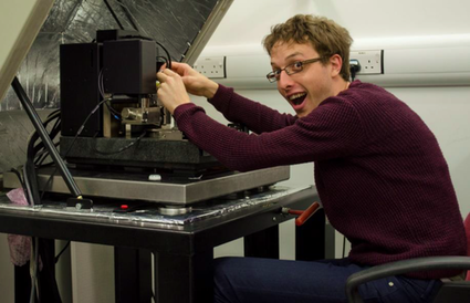
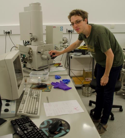
My part of this project is investigating the surface morphology of some of Anvil’s SiC and the influence this has on the cubic GaN layers that are grown on them here in Cambridge. I do this through atomic force microscopy, scanning electron microscopy and scanning capacitance microscopy. I hope to stay with the group for my PhD, but I’ll be working on a different aspect of LED research.
What do you like best about working in the group?
It’s so friendly! I really felt like I belonged here in about a week, which is certainly not true of every workplace. There is a lot of laughter in the office and we have cake together once a week, which definitely helps with this. I’m also really happy that the group puts so much emphasis on teaching and outreach and am looking forward to getting involved in this.
Where do you see nitrides in future?
My area of nitride research is in LEDs where there has already been a big impact in lowering power consumption for lighting. The biggest challenge here is to fill the “green gap” by creating energy efficient green LEDs. This opens the door to LED displays that do not require LCDs or other modulators, as well as creating efficient lighting with a warmer colour, closer to the tungsten light bulbs that we are used to. I see a future where every light bulb and every display uses nitride LEDs: in the home, in streetlights, even lighting for live events and film. All this has big potential to save energy. There is also potential to make cheap, portable UV sterilisation lamps that could transform health in parts of the world without proper sanitation, which is an application that has huge potential to improve lives.

UPDATE:
Peter has completed his MRes and returned to the GaN group to start a PhD in October 2016, looking at porous GaN in LEDs. See his homepage here.
