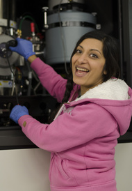
Dr Lata Sahonta

Lata talks about her research, her role in the group and the future of GaN.
Download Lata's researcher profile as a PDF
How did you join the Cambridge Centre for Gallium Nitride?
I became familiar with the Cambridge Centre for Gallium Nitride during my PhD at Bristol University, where I investigated UV LED and laser structures by TEM, in collaboration with Hiro Amano's team at Meijo University in Nagoya. I often attended conferences where the Cambridge GaN team were presenting exciting new results, and I had lots of useful discussions with Cambridge students.
During my Marie Curie Fellowship, Colin Humphreys was a co-investigator in our very large European research consortium to study the nano-scale properties of low-dimensional nitride materials such as quantum dots and nanowires, and I was occasionally invited by Colin to give talks at the Cambridge Centre for Gallium Nitride about my work. I was living in Greece and was hoping to continue my research work there or elsewhere in Europe, but my lovely scientist boyfriend (now husband) lived in Cambridge and was very keen for me to join him. So I took a postdoctoral job in the Device Materials Group at the Department of Materials, working on functional oxides for multiferroic devices.

I was excited to be back in the UK and to study a new materials system but I was still really interested in nitride materials, so I did a few short collaborative experiments with some of the GaN group's members in my spare time. After a few months of being in the UK, Colin told me that the Cambridge Centre for Gallium Nitride had received a very large EPSRC Programme Grant to investigate factors that limit the efficiency of blue LEDs, and encouraged me to apply as the microscopist on the grant. I'm really glad that I kept up my enthusiasm for studying gallium nitride despite having moved into a new research field, since my interest in the group's ongoing work must have really helped me to get the job.
What is your role in the GaN Group?
Nitride crystal films contain many complicated crystalline defects, so using electron microscopy is a good way to find out about their structure and chemical makeup. On a typical day I perform a variety of different TEM experiments which help to learn about how the crystalline structure of gallium nitride affects its optical and electrical properties. The TEM fires an intense electron beam at a thin sample of the crystalline material being studied, and the electrons diffract as they pass through. Any defects in the crystal scatter the electrons differently from the perfect regions of crystal, so we can learn how many defects are present, what shape they are, how they are created, and how we might be able to eliminate them, or at least move them around in the crystal so that they are less harmful to device properties.
As well as doing experiments, I train new students to operate the TEMs, and how to interpret results and use software to process TEM images. I also teach a spectroscopy course to under-graduates, and I supervise and mentor both undergraduates and graduate students, which is great fun and very rewarding.

What do you like best about working in the Group?
I really like that we have such great facilities in the Department of Materials; I can study the exact atomic stacking sequences in a quantum well, or the elemental composition of an LED structure, or investigate defects in a gate channel in a nitride transistor, all using a beam of electrons accelerated to 75 % light speed!
I also really like the cooperation in the group; we are encouraged to talk about our results often with other group members, and we all work together to spread the workload of experiments so that we can get as much information as possible about a particular materials problem, or to improve material properties that will enable progress in device development.
Where do you see gallium nitride in the future?
Despite 2014's Nobel Prize, gallium nitride is still the most useful material that nobody's ever heard of, but that will steadily change with more public engagement from the nitride research community. Currently none of my family or non-physicist friends know what gallium nitride is, but all of them rely heavily on many different kinds of nitride devices in their everyday lives. It's really important that the public see gallium nitride as an energy-saving yet highly enabling technology for white lighting, information transmission and processing, as a potential method of water purification, and increasingly for power electronics as we demand higher data rates. The great thing is that the as we continue to improve GaN-on-silicon device fabrication, the benefits of nitride technology will far outweigh the relatively low cost. This will allow gallium nitride applications to improve the lives of everyone, whilst reducing the harmful impact that current lighting and power electronics systems have on the environment.
