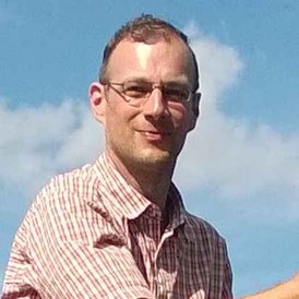
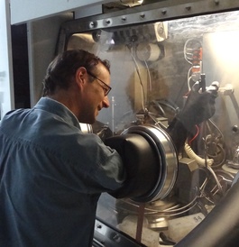
Dr Markus Pristovsek

Markus talks about his career, his role in the group and his vision for the future of GaN.
Download Markus' researcher profile as a pdf.
How did you join the Cambridge Centre for Gallium Nitride?

I joined the centre in autumn 2012 just two months after I met Colin Humphreys and Rachel Oliver at a conference in St. Petersburg. I helped to set up the second 6x2” MOVPE reactor and use it to make semi-polar LEDs. My work on semiconductors is split between earlier work in Berlin starting in 1993 on GaAs and related materials and nitride semiconductors since 2004. My main topic has been to understand the growth i.e. making the semiconductor and related nanostructures. In the mid-90s we developed in Berlin the optical control technology now sold by the company LayTec. After my PhD (on exotic non-(001) surfaces of GaAs) I spent more than two years in Japan literally watching InAs quantum dots growing in a growth chamber with a scanning tunnelling microscope inside (“in-situ STM”). After another year at a research centre in Berlin I went back to the Technical University Berlin, as non-permanent Associate Professor. There I realised the one and so far only in-situ STM for MOVPE growth (the industrial production method for semiconductor nanostructures) and also studied InN growth. After the head of the group retired in 2006, the nitrides became the main focus, and I continue that work in Cambridge.

What is your role in the GaN group?
My position is Senior Research Associate, so I am paid for doing research. Cambridge is a privileged place. Hence, I can choose what and how much I want to teach (since there are many eager post-docs around). So I am in the laboratories a lot (much more than in the last 10 years before). There I produce LEDs and other nanostructures in the MOVPE growth system and analyse them too. One current topic is to find out what limits the efficiencies of LEDs.
What do you like best about working in the group?
That we are so many post-docs from many countries in one place, while at the same time the atmosphere is that of a university which promotes free thinking and creativity. And getting a transmission microscopy image within a week or two was a new experience for me. Not to forget, that Cambridge is a great place to live and raise a family.
Where do you see nitrides in future?
Nitrides have become quite mature (mostly driven by brute force optimisation). They are the second largest semiconductor business after silicon. Still, fundamental limitations (why are green LEDs not as good as blue?) require a better understanding to tackle them. Further in the future, hybrid materials are quite a possibility. Since GaN is transparent, a good light emitter, and biocompatible, this may be biologic-electronic-photonic hybrid circuits.
