Occasional writer for the IOP's Physics World.

Porous GaN
The research during my PhD was focused on the development of porous GaN devices. I was using nanoscale porosity to engineer material performance for electrical and optical devices, such as LEDs and sensors.
Distributed Bragg Reflectors (DBRs)
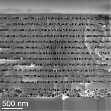
We have developed an electrochemical etching process that targets conductive regions of GaN to form nanopores. This has been demonstrated by forming layered distributed Bragg reflectors (DBRs). A scanning electron microscope (SEM) image of such a layered porous GaN DBR is shown (right).
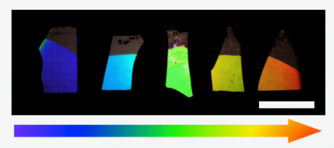
The large difference of refractive index between porous GaN and bulk GaN can be used to create a highly reflective structure, which does not introduce strain. By varying the thicknesses of the layers the peak reflected wavelength can be tuned.
The photo below shows the range in reflected colour that we have created in porous DBRs.

For UV light sources
Porous GaN also has implications for Ultra-violet (UV) light sources. UV emitting devices have much lower efficiency than their blue counterparts. Efficient UV emitters would be transformative to sterilisation methods, allowing cheap, portable systems for hospitals and water treatment that could reach places where there are currently no effective sterilisation methods. My research aims to improve UV LED efficiency by using an active region with nanoscopic porosity. Localisation in the porous regions should reduce carrier diffusion to non-radiative recombination centres and increase the radiative recombination efficiency. In addition, quantum size effects will shift light emission towards the UV, meaning lower Al content would be required, bypassing several problems with high Al content AlGaN as an emitter.
Sensors
My work also included development of porous GaN for a variety of uses in sensors, where I was looking to exploit its high surface area and high thermal insulation.
Previous Education
After gaining a first class MEng in Electronic and Electrical Engineering at Imperial College London I came to Cambridge under the Centre for Doctoral Training in Integrated Photonic and Electronic systems (IPES CDT), run jointly with UCL. In the first year of the course I completed two research project as part of an MRes, the second of which was with the Cambridge Centre for Gallium Nitride.


