 A steady increase in world energy demands combined with the depletion of fossil fuels is driving research into cheaper and more energy-efficient solid state lighting and photovoltaics. III-nitride devices offer low power consumption, whilst maintaining high device performance, as demonstrated by the commercial success of InGaN/GaN blue light-emitting diode (LEDs).
Cost is probably the major factor limiting the widespread use of white LEDs in homes and offices. GaN-based LEDs are significantly more expensive than filament light bulbs or CFLs. However, the cost is continuously decreasing. It should be noted that the total ownership cost of lighting includes energy savings and replacement cost, which makes LEDs much more competitive, compared to conventional lighting technologies. Nevertheless, to achieve significant market penetration, the initial cost (per kilolumen) of LEDs needs to be reduced by a factor of 10 to be comparable to the cost of CFLs. To achieve the required cost reduction, many aspects of the manufacturing process will need to be addressed in parallel. Considering the material growth (the first step in manufacturing LEDs), increasing the diameter of the currently used substrates, 50-mm-diameter sapphire (Al2O3) and SiC, will reduce costs by increasing the usable wafer area.
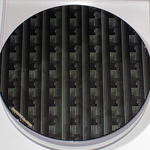
 A more dramatic cost reduction might be achieved by growing GaN-based LEDs on silicon wafers, which have the advantage of being readily available in large diameters (e.g., 150 mm or larger) and at low cost. In addition, such wafers are compatible with existing processing lines commonly used in the electronics industry. There are several significant technological challenges in growing GaN on Si substrates, and we are doing research into overcoming the difficulties of nitride growth on silicon.
To achieve high performance LED devices when grown on Si substrates, we need to address the high dislocation density and wafer cracking issues arising from the lattice parameter and thermal expansion mismatch between GaN and Si. Fortunately, we can control the thermal stress in GaN films on silicon by the use of AlN and AlGaN intermediate layers. The lower lattice parameter of AlN forces the GaN to be deposited in compression, counteracting the thermal tensile stress acting from the silicon substrate. We use a silicon nitride interlayer to reduce the density of threading dislocations, by encouraging them to bend into the (0001)-plane and move laterally where they annihilate with dislocations of opposite Burgers vector.


