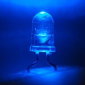
LEDs: Lighting the Future
Next time you change a tungsten filament light-bulb, give a brief thought to the amount of energy that bulb will have used up over its lifetime: more than 200 million Joules. (This is about the same amount of energy as is contained in 3 tonnes of coal!) If you consider how many light bulbs must be in use in the world at this moment, it becomes clear that a huge amount of energy is spent keeping our homes and offices lit. In fact, about a fifth of electricity usage in the UK is for lighting. Hence, improvements in something as simple as light bulb efficiency could have an enormous impact on the UK’s greenhouse gas emissions and use of fossil fuels.

A new semiconductor material – gallium nitride (GaN) – provides a potential solution to the lighting problem. GaN is used to make white light-emitting diodes (LEDs). These solid state-light sources are already much more efficient than conventional tungsten filament light bulbs, and could potentially yield efficiency improvements of more than ten times (and be three times more efficient than compact fluorescent lamps). To achieve these vast improvements in efficiency, we need to thoroughly understand the material from which we make the LEDs, and how its structure, composition and properties influence LED performance. We also need to design devices which make the best possible use of everything we learn about the material. A large number of different factors influence the efficiency of LEDs, and in this programme, scientists from Cambridge, Manchester, Bath and Strathclyde are pooling their expertise to understand what limits the efficiency and find solutions which will benefit all of us, by providing sensibly-priced, highly-efficient lighting units which will be long-lasting and provide attractive high-quality light in homes and offices.

To do this, we are breaking down the question of LED efficiency into a number of inter-linked scientific projects. GaN LEDs are based on thin layers of material grown on other materials such as silicon or sapphire. Electric current is passed into the active region of the LED, from which the light is emitted. The active region consists of very thin alternating layers of GaN and another semiconductor – indium gallium nitride (InGaN). The InGaN layers are only ten atomic layers thick and are called quantum wells. In the InGaN layers, positive and negative charge carriers become trapped and hence combine with one another giving out light. The GaN and InGaN crystals are not perfect, however, and defects in their structure can disrupt the light emission process, resulting in the production of heat rather than light and a reduction in LED efficiency. In the early years of our programme, we plan to tackle fundamental questions relating to light emission efficiency, by pursuing projects concentrating on the defects in the material, the detailed small-scale structure of the InGaN quantum wells and the electric fields which arise in those quantum wells. The effect of all of these factors will be dependent on the amount of electricity injected into the LED, and a major problem is that LED efficiency drops at high injection currents. Since high brightness LEDs for lighting require high electric currents, we will also need to understand this question before solid state lighting can reach its full potential.

The new materials and structures we develop will have to be integrated into working LED devices, and the architecture of those devices is also a key factor affecting efficiency. Hence, another of our research projects will address device design. By bringing the new ideas we develop about materials and devices together we aim to produce LEDs that are highly efficient and thus beneficial to our environment, cheap to buy and, unlike compact fluorescent lamps, produce an attractive colour of light to make homes and offices pleasant and healthy places to be. In the end, we hope the products of our research really will be lighting your future!
