PowerGaN: Nitrides for HEMTs
Most power electronics devices realized in the GaN power fields are presently limited to 600-900V, however, understanding reliability of those devices and failure mechanisms and what limits this maximum voltage is unclear. Pathways need to be found to open the market to even higher voltages, which would also benefit reliability of below 600-900V devices due to reduced degradation acceleration factors. Our work is addressing these challenges.
Devi

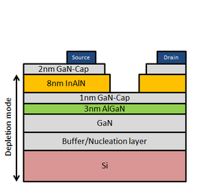
ces being grown, characterised, processed and tested include normally-on HFET device structures which are designed with suitable process etch stop layers/barriers. These form the basis of very low risk but potentially very high performance recessed gate normally off MOS-HFETs. These devices lead to novel normally-off integrated Cascode switches which benefit from the superior performance of a normally-on device. A different but potentially very high performance type of device that also evolves from the conventional HFET structure is a normally off Schottky Source/Drain tunnel junction HFET. The lateral device structures address the low power and medium power sectors (consumer electronics, IT, etc.). Vertical structures meet the requirements for higher power.
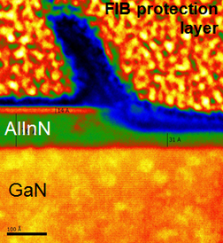
The Cambridge group focuses on MOCVD growth and characterisation of lateral and vertical power and RF GaN electronics. These are grown on a variety of substrates including large-area Si, SiC, free-standing GaN and sapphire, with a view towards moving to even larger area Si in the future to support the growing demand for low-cost, high-power devices. Characterisation work involves XRD, CL, AFM, CV profiling and with a particular focus on TEM analysis of interfaces and compositions within device layers.

