Multimicroscopy of Nitrides

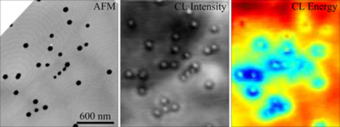
The commercial market for electronic and optoelectronic devices based on nitride semiconductors is growing extremely fast, but the fundamental science underlying these devices is lagging behind. In this project, MACONS, we are exploring the vital link between structure and properties in nitride materials, in order to reveal the limitations of current devices and to pave the way for new, improved technology. The key strategy of the project is to combine multiple microscopy techniques to develop a comprehensive understanding of nanostructures and defects in the nitrides, and to link these discoveries to nanoscale measurements of the optical and electrical properties. This requires a synergy of different techniques, ranging from techniques commonly used on metals (such as atom probe

tomography) to techniques which focus exclusively on semiconductors (such as scanning capacitance microscopy). It also requires the development of new approaches to the application of these techniques, to allow the same nanoscale regions of material to be assessed in multiple microscopes, so that the structure and composition of a specific nanostructure may be linked directly and unambiguously to its electrical and optical properties. Overall, the aim is to provide a much more complete picture of nitride materials science than has ever previously been achieved, and to apply this new understanding to engineering improved materials for nitride optoelectronic devices.

