Integration of RF Circuits with High Speed GaN Switching on Silicon Substrates
Future generation wireless communication systems will demand high data rate modulation schemes with both a large modulation bandwidth and a high Peak to Average Power Ratio (PAPR). This presents a major Radio Frequency Power Amplifier (FRPA) design challenge when targeting the conflicting system requirement of high efficiency and high linearity. The Doherty Amplifier is employed almost exclusively in current 3G/4G macro based-stations. Operating at peak powers >100 Watts, this approach allows relatively high efficiency to be maintained over typically 6-9dB PAPR, with high linearity achieved through the aggressive use of digital pre-distortion (DPD). Moving to 5G systems will certainly involve a reduced reliance on large macro base-stations, with small-cell base-stations (typically operating at low peak power levels <10’s of Watts) becoming commonplace. However, the overall network power consumption is expected to increase significantly as a result of densification and high efficiency operation will remain a priority.
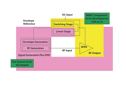
Fig.1 Envelop Tracking (ET) Radio Frequency Power Amplifier (RFPA) architecture.
Envelope Tracking/Restoration (ET/ER) RFPA (Fig.1) is becoming a key technique in RF amplifier designs where it enables both efficient and linear amplification of modulated signals with high PAPRs. This is achieved by varying the broadband RFPA output bias voltage using a very efficient DC-to-DC converter, the envelope modulator, in synchronisation with the amplitude variation of the modulated RF input signal (Fig. 2).
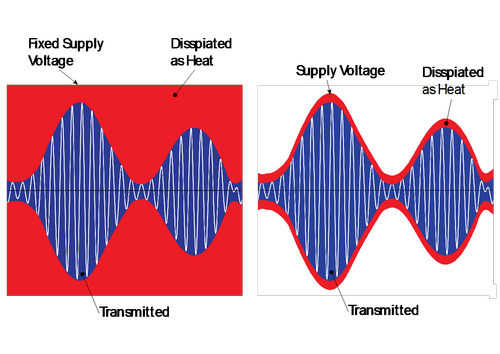
Fig.2 Envelop Tracking waveform, illustrating the power wasted in a radio transmitter without (left) and with (right) the use of Envelope Tracking technology.
The aim of the project is to develop a GaN-on-Silicon technology platform that allows integration of RF and Power converter functionality for a range of high efficiency/high frequency applications. Exploiting the unique characteristics of GaN-based HEMTs, very efficient DC-to-DC variable voltage converters will be designed and built to modulate the drain bias voltage to broadband Radio Frequency Power Amplifiers (RFPA), ensuring that the RFPA remains in an efficient compressed mode of operation while still providing linear amplification. When targeting 4G/5G base station applications, the key challenge is that the DC-to-DC converter element must operate at very high speeds/bandwidth, necessitating integrated solutions.
GaN-on-Si is the ideal material platform to achieve this objective, providing a low cost device technology for both the novel integrated fast converter module and the RFPA. Since parasitic elements will limit the speed/bandwidth of both functions, full Monolithic Microwave Integrated Circuits (MMICs) integration with novel architectures and optimised high resistivity buffer layers will be required.
To deliver the aims of this ambitious project, a consortium has been formed to bring together the leading UK groups with vertically integrated expertise in crystal growth (University of Cambridge), device design and fabrication (University of Sheffield), MMIC design and fabrication (University of Glasgow), converter design (University of Manchester) and large signal RF characterisation and PA design (Cardiff University).
Material challenges: The research carried out at the Cambridge Centre for Gallium Nitride will focus on the development of a common epitaxy platform that is suitable for both the power switch and RF power amplifier elements of an integrated envelope tracking circuit. This will require optimisation of the GaN-on-Si epitaxy stack to give a high performance two-dimensional electron gas (2DEG), whilst controlling losses due to any conduction in the buffer layers and also controlling electron traps which lead to current collapse phenomena and device breakdown.

