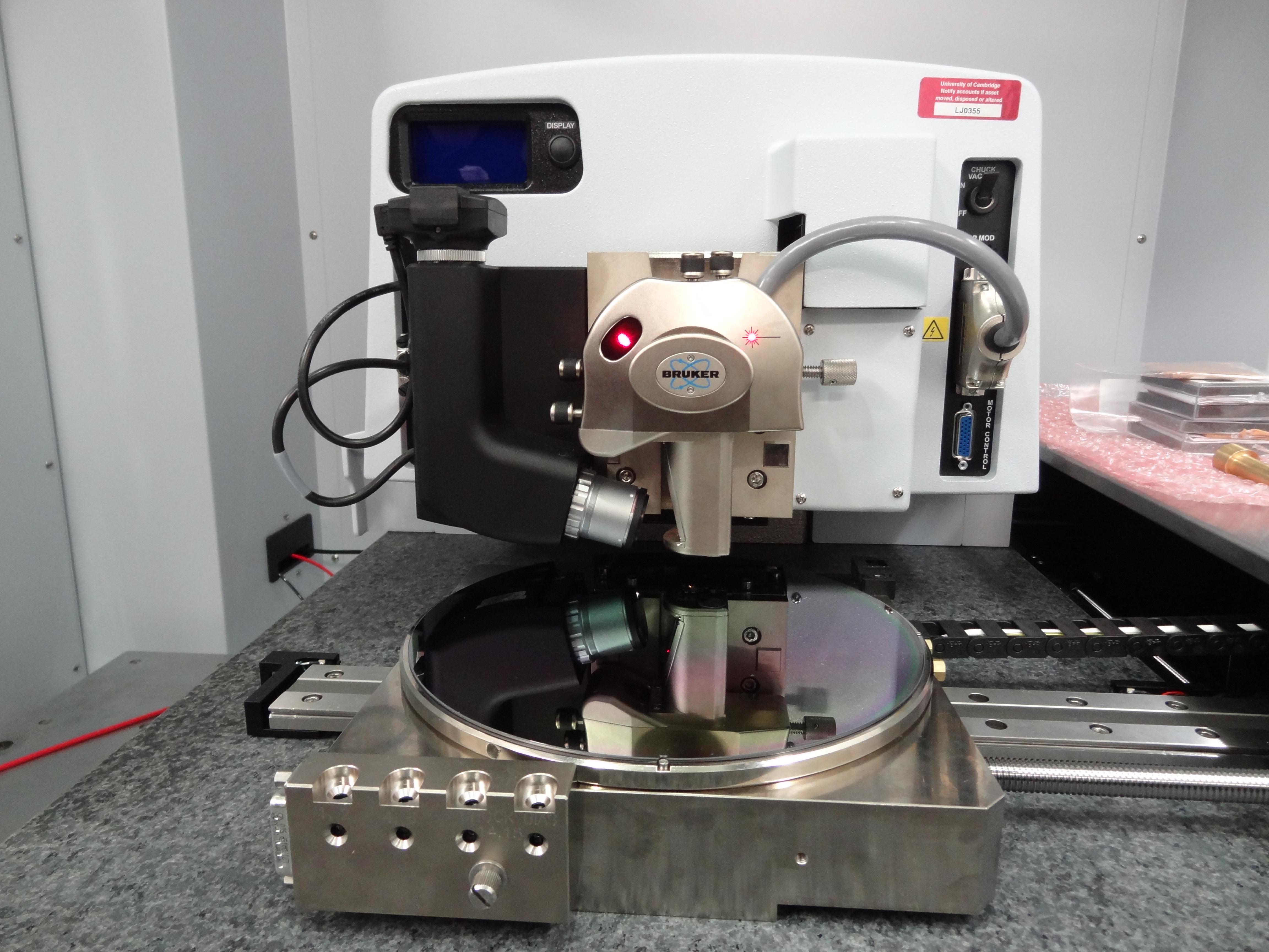
The image shows an 8" GaN-on-Si wafer from our Veeco large wafer reactor being imaged on the 8" stage of our new Bruker Nano Surfaces Dimension Icon Pro AFM. We even have automated mapping capability to efficiently sample morphologies and materials properties across the wafer! This is an exciting development for the production of GaN devices.
The AFM is part of the Cambridge spoke of the Sir Henry Royce Institute. Read more about how we use it here.